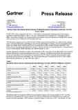
.2011 – Worldwide semiconductor capital equipment spending is expected to total $35.2 billion in 2012, a 19.2 per cent decline from projected 2011 spending of $43.5 billion, according to Gartner, Inc. Excess electronics inventory and poor demand as a result of the slowing macro economy are to blame for the declining spending.
“The slowdown appears to be across the board. While it appears the foundries will continue their capacity race at 28 nanometers (nm), spending on 45 to 90 nm technologies is slowing, and some equipment from those technology nodes is being used for 28 nm production to help increase capacity utilisation,” said Klaus Rinnen, managing vice president at Gartner. “Due to weaker-than-expected growth in the production units of media tablets, NAND spending has softened slightly as well.”
Gartner expects the slowdown to last for the remainder of 2011 and into the first half of 2012. By mid-2012 Gartner expects the supply and demand to be more in balance, so DRAM and foundry will need to begin to increase spending to meet an increase in demand as the PC market rebounds and consumers begin spending once the economy stabilises a bit. The next growth year is expected to be 2013, when capital spending will increase by 18.4 per cent (see Table 1).
Worldwide wafer fab equipment (WFE) revenue started slowing in the second quarter of 2011, and the decline will accelerate in the second half of 2011 with the added pressure of slowing device sales and excess inventory liquidation. WFE revenue is forecast to grow 9.4 per cent in 2011, but decline 19.6 per cent in 2012. The need for leading-edge equipment is benefiting immersion lithography, etch, certain segments in deposition involved in double patterning, and critical leading-edge logic processes. Leading edge is not the only benefactor of expanding mobile media markets. Analogue and discrete devices needed for power management and energy management will drive the need for 200-millimeter (mm) equipment.
Worldwide packaging and assembly equipment (PAE) revenue is projected to decline 1.4 per cent in 2011 and decrease 17.5 per cent in 2012. Orders for PAE have softened more aggressively than previously expected as supply comes in line with expectations. For back-end process providers- capital expenditure (capex) purchases, 3D packaging and copper wire bonding for lower-cost solutions will still be the focus, but at a reduced pace. Most major tool segments will see slightly negative sales in 2011, but advanced tooling will once again be stronger than the general market this year. For 2012, traditional tooling segments will see a sizable decline in sales, while advanced packaging segments are expected to fall less than traditional when compared with 2011.
For 2011, the automated test equipment (ATE) market is expected to remain essentially flat with revenue growth at 0.4 per cent. The market has been driven by the continued demand of system-on-chip and the advanced radio frequency segments of the market. Memory ATE will likely pull back in 2011 as DRAM capex softens. However, NAND testing platforms are expected to be stronger than the general memory test market this year. For 2012, analysts expect a significant decline in tester sales, though memory systems should hold up reasonably well compared with most cycles as DRAM capex returns.
Additional information is available in the Gartner report “Forecast Analysis: Semiconductor Manufacturing Equipment, Worldwide, 2010-2015, 3Q11 Update.” The report is available on Gartner-s website at http://www.gartner.com/resId=1801517.
This research is produced by Gartner-s Semiconductor Manufacturing programme. This research programme, which is part of the overall semiconductor research group, provides a comprehensive view of the entire semiconductor industry, from manufacturing to device and application market trends. More information on Gartner-s semiconductor research can be found in the Gartner Semiconductor Manufacturing Focus Area at http://www.gartner.com/technology/core/products/research/markets/semiconductorManufacturing.jsp.
Gartner, Inc. (NYSE: IT) is the world-s leading information technology research and advisory company. Gartner delivers the technology-related insight necessary for its clients to make the right decisions, every day. From CIOs and senior IT leaders in corporations and government agencies, to business leaders in high-tech and telecom enterprises and professional services firms, to technology investors, Gartner is the valuable partner to 60,000 clients in 11,000 distinct organizations. Through the resources of Gartner Research, Gartner Executive Programs, Gartner Consulting and Gartner Events, Gartner works with every client to research, analyze and interpret the business of IT within the context of their individual role. Founded in 1979, Gartner is headquartered in Stamford, Connecticut, U.S.A., and has 4,400 associates, including 1,200 research analysts and consultants, and clients in 85 countries. For more information, visit www.gartner.com.


You must be logged in to post a comment Login